Field Effect Transistors (FETs)
1. Fundamentals
Core Concept A voltage-controlled current source. Ideally, the Gate draws zero DC current (Infinite Input Impedance). In reality, there is tiny leakage and gate capacitance, so current flows briefly during switching.
Key Definitions
- VGS (Gate-Source Voltage): The "Valve." Controls how wide the channel opens.
- VDS (Drain-Source Voltage): The "Pressure." Pushes current through the channel.
- Vth (Threshold Voltage): The specific VGS where the channel turns ON.
- IDSS (Saturation Current): The max current a JFET/Depletion FET flows when VGS=0.
Core Equations
- Current (Saturation): ID = k · (VGS - Vth)²
- Transconductance: gm = ID / VGS
- Gain (Common Source): Av = -gm · RD
2. MOSFET Operation
🎛️ Interactive Region Explorer
Vgs (1V) < Vth. Channel is closed.
Enhancement vs Depletion
- Enhancement Mode (Normally OFF):
- If VGS < Vth, no channel exists (IDS=0).
- You must apply bias to turn it ON. (Standard for logic/power).
- Depletion Mode (Normally ON):
- The channel exists at VGS=0.
- You need a Negative bias on the Gate to stop current flow.
- Max current flows when VGS=0.
Regions of Operation (N-Channel)
-
Cutoff (Open Switch)
- Condition: VGS < Vth.
- Result: IDS ≈ 0. The switch is OFF.
-
Ohmic / Linear (Resistor)
- Condition: VGS > Vth AND VDS is small.
- Behavior: Acts like a voltage-controlled resistor.
- As VDS increases, ID increases linearly (I = V/R).
- Use Case: Variable resistors, Power switching (minimize heat).
-
Active / Saturation (Current Source)
- Condition: VDS >= (VGS - Vth).
- Behavior: Acts as a constant current source.
- The channel is "pinched off" at the drain. Increasing VDS does not increase current. Current is determined only by the Gate drive (VGS).
3. JFETs & Depletion Mode
JFETs are Normally ON. They act like the "Reverse" of an Enhancement MOSFET.
How JFETs Work
- At 0V bias, maximum current flows (I ≈ IDSS).
- As you apply Negative voltage to the gate, the channel pinches off.
- Critical Warning: The Gate is a diode junction to the channel. Never forward bias it (don't make Gate positive vs Source) or you will conduct current and destroy it.
JFET vs Depletion MOSFET
- Similarities: Both are Normally ON. Both turn off with negative VGS.
- Differences: Depletion MOSFETs have an insulated gate, so you can drive the gate positive (to get even more current) without damage.
- Why use JFETs? They are excellent for Low Noise linear applications (audio front-ends, amplifiers) and are less susceptible to ESD than MOSFETs (no oxide layer to puncture).
4. Design Intuition: Source vs Drain
MOSFET structure is symmetric. The "Source" and "Drain" labels are determined by the voltage potentials, not the package.
The Rule
- N-Channel Source: Whichever terminal has the Lower voltage.
- P-Channel Source: Whichever terminal has the Higher voltage.
The "Negative Drain" Trap (Example)
Imagine an N-MOSFET switching a line to Ground.
- You assume the Drain is the high side and Gate = 0V turns it off.
- Scenario: The "Drain" line goes negative (e.g., -2V).
- Reality: That "Drain" terminal is now lower voltage than the Source (GND). It becomes the True Source.
- Calculation: VGS = VG - VTrueSource = 0V - (-2V) = +2V.
- Result: The FET turns ON unintentionally!
- Fix: To keep it off, the Gate must be more negative than the most negative signal.
5. Applications
1. High-Z Buffers & Source Followers
- Used where BJT input current would load down the source.
- Gain Formula: Av = 1 / (1 + 1 / (gm · RL))
- Impedance Issue: Output Z is 1/gm. Since gm changes with signal current, Output Z "wobbles," causing distortion.
- Fix: Use a constant current source load or negative supply to stabilize the operation point.
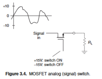
2. Analog Switches
- FETs in the Ohmic region act as low-resistance switches. Used in multiplexers and sample-and-hold circuits.
3. Variable Resistors
- In the Ohmic region, changing VGS changes RDS. You can use this for voltage-controlled volume control (limiting factors apply).
4. Power Switching
- MOSFETs dominate here due to low RDS(on) and resistive nature (easy to parallel).
6. Analog Signal Switching
Detailed considerations for using FETs to switch audio/data signals.
The Feedthrough Problem
Ideally, an OFF switch is an air gap. In reality, a MOSFET has Drain-Source Capacitance (Cds).
- Effect: High-frequency signals jump across the capacitor, appearing at the output even when the switch is OFF.
- Solution: Use a "T-Switch" or SPDT configuration to ground the signal path when OFF.
The Floating Output (Ghost Signals)
If the switch output is floating (High-Z), it picks up noise/leakage easily.
- Resistor Fix: Add a load resistor to ground (1kΩ - 100kΩ).
- Too Low (1k): Kills feedthrough, but creates a voltage divider with Ron (Signal loss).
- Too High (1M): No signal loss, but too weak to drain capacitive leakage.
- Best Fix: Use a second switch (SPDT) to actively ground the output when the signal is disconnected.
The CMOS Transmission Gate
Problem: An N-MOS passes "Low" well but chokes on "High" signals (as Source voltage rises, VGS drops, turning it off). A P-MOS does the opposite. Solution: Put an N-MOS and P-MOS in parallel.
- One handles the low voltages, the other handles the high voltages.
- This allows Rail-to-Rail switching.
Distortion & Charge Injection
- THD (Distortion): Ron varies as the signal voltage changes (since VGS effectively changes). This non-linear resistance creates distortion in audio.
- Charge Injection: When the switch turns OFF, the charge stored in the Gate capacitance has to go somewhere. It often squirts out into the signal path, causing voltage spikes.
- Fix: Use specialized "Low Charge Injection" analog switch ICs.
7. Current Sinks & Sources
Definition: Circuits that draw (sink) or push (source) a specified current regardless of the voltage at that node.
Why use a Current Sink?
Imagine an Emitter Follower where you want to draw a fixed current X from the emitter.
- Resistor Method: You could just use a resistor to the negative rail.
- Problem: Requires more power dissipation and reduces input impedance.
- Active Sink Method: Using a JFET or BJT maintains high impedance and precision.
The JFET Current Sink (Example)
Since JFETs are depletion mode (On at 0V), we can self-bias them.
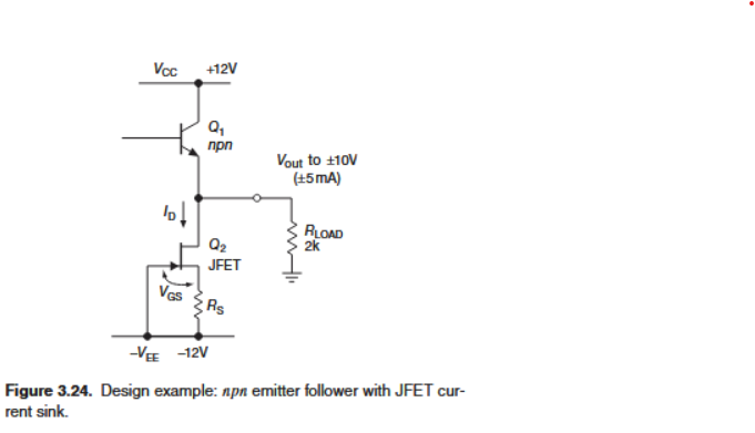
- Setup: Gate tied to -12V. Source tied to -12V + (ID · RS).
- The Math: VGS = VG - VS = -12 - (-12 + IDRS) = -IDRS.
- Design: You select RS such that the VGS drop gives you the exact current you want.
- Formula: RS = VGS(required) / 5mA.
Cons of JFET Sinks: You cannot easily predict ID because IDSS varies wildly between parts. It is not consistent enough for tight tolerances. Better to use a BJT sink.
The BJT Current Sink / Mirror
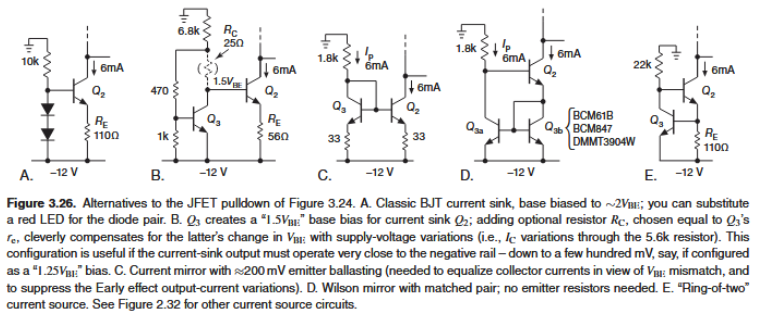
- Concept: You specify the collector current by sinking a fixed amount at the emitter.
- Benefit: You don't need precise VBE biasing. The collector current will roughly equal the emitter current you set.
- Common Emitter Application: Placing a current sink in the emitter sets a nearly constant IE (and therefore IC).
- The DC collector voltage becomes: VC ≈ VCC - (Isink · RC).
- This decouples the bias point from the transistor's Beta and VBE.
8. Gate Drive Dynamics
This section matters for switching, motor drivers, and power supplies.
A. Static Gate Current (The Leakage)
- The Ideal: The Gate is isolated by glass. IG = 0.
- The Reality: Tiny pico-amp leakage exists.
- Protection Diodes: Many discrete MOSFETs have built-in Zener diodes for ESD protection. These leak much more (nano-amps/micro-amps).
- Lesson: Do not use generic protected MOSFETs for ultra-high impedance electrometer circuits.
B. Dynamic Gate Current (The Bucket)
Think of the Gate as a Bucket (Capacitor), not a switch.
- DC: Once the bucket is full, no more water flows.
- AC (Switching): To turn ON, you must fill the bucket. To turn OFF, you must dump it.
- The Math: I = Qgate / time.
- Example: If Qg = 50nC and you want to switch in 100ns:
- I = 50nC / 100ns = 0.5 Amps.
- Takeaway: You need a dedicated Gate Driver Chip to provide these high current spikes. A standard GPIO pin (20mA) is too weak to switch fast.
C. The Miller Effect (The Plateau)
As you charge the gate, the voltage rises, stops (flat), then rises again.
- Region 1 (Charging CGS): Voltage rises linearly. MOSFET is OFF.
- Region 2 (The Miller Plateau): MOSFET turns ON. Drain voltage drops.
- The falling Drain "sucks" charge away from the Gate via the Gate-Drain Capacitor (Cgd).
- You keep pumping current in, but voltage stays flat because the feedback capacitor eats it all.
- Region 3 (Saturation): Switching is done. Voltage rises to driver level.
Why it matters: During the plateau, the MOSFET is half-on/half-off (Acting as a resistor). It gets HOT. You want to blast enough current to push through this plateau ASAP.
9. Circuit Analysis: Feedback Pairs
This circuit combines the best of both worlds: JFETs (High Input Z) and BJTs (High Gain).
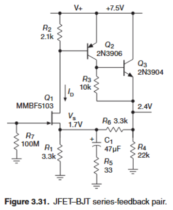
Block 1: Input Stage (JFET)
- Role: Provides extremely high Input Impedance.
- Current: ID is dictated by the source resistor (R2).
Block 2: Gain Stage (BJT Q2)
- Role: High Gain Amplifier.
- Bias: Collector is biased by R3 to a certain current.
- Gain Formula: Gain ≈ gm · RLoad
Block 3: Output Stage (BJT Q3 - Emitter Follower)
- Role: Buffer. High Input Z, Low Output Z.
- Why it matters: Q3 pulls very little current from Q2.
- Without Q3: The load (e.g., 3.3kΩ) would appear in parallel with Q2's collector, dragging the gain "into the gutter."
- With Q3: The load is isolated. Q2 sees a high impedance, so the gain "skyrockets."
10. Advanced JFET Circuits
A. Hybrid JFET / Op-Amp Amplifier
(Reference: Art of Electronics Fig 3.34)
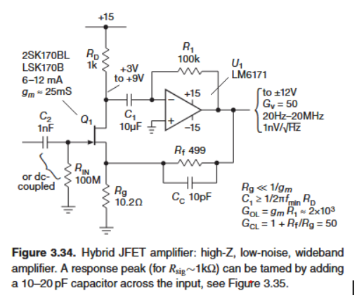
Open Loop Analysis (No Rf)
- You bias your JFET, and an AC current ID flows.
- The Op-Amp is a Current-to-Voltage converter.
- Output: Vout = gm · Rgain.
- Example: If gm = 25mS and R = 100k, Gain = 2500. A 1mV input creates 2.5V output.
Closed Loop (Negative Feedback)
- Mechanism: If Input $\uparrow$ $\to$ JFET turns on harder (VGS closer to 0) $\to$ Op-Amp Output $\uparrow$ $\to$ Current into Source $\uparrow$ $\to$ VSource $\uparrow$.
- VG and VS increase together, so VGS stays constant.
- Result: The gain is now set by the feedback resistors (Rf / Rg), not the transistor parameters.
B. JFET Differential Amplifiers
(Reference: Art of Electronics Fig 3.36)
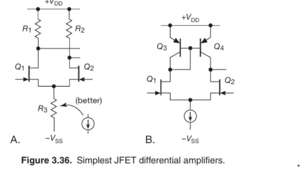
Circuit A: Resistive Load
- Current Sink: Sets the total current for the pair.
- Steering: If VQ1 > VQ2, Q1 pulls more current. Since the total is fixed, Q2 must pull less.
- Result: Voltage at D1 drops, Voltage at D2 rises. The difference is amplified.
- Common Mode: If both inputs rise by 1V, they "fight" for current equally. No change in output.
- Issue: Very little gain; variation in gm between parts.
Circuit B: Active Load (Current Mirror)
- Replaces the drain resistors with a BJT Current Mirror (Q3 & Q4).
- The mirror acts as a Constant Current Source (High Resistance).
- Result: High Gain. Since Gain = gm · Rload, and the mirror provides a huge Rload, the gain increases significantly.
C. JFET Diff Amp with Feedback
(Reference: Art of Electronics Fig 3.37)
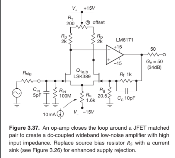
- Setup: A current sink (e.g., 10mA) sets the total current.
- Initial State: Vin = 0. Q1 and Q2 share current equally (5mA each). No differential output.
- Signal Applied: If Q1 Input rises, Q1 conducts more. Q2 conducts less. This difference is amplified.
- Feedback: The negative feedback loop limits this amplified difference to a manageable gain, stabilizing the circuit against gm variations.
11. Power MOSFET Specifics
Detailed requirements for driving high-current devices.
Thermal Stability (Rds(on) vs Temp)
- Relationship: Rds(on) increases with temperature (Positive Temp Coefficient).
- The Benefit: MOSFETs are thermally stable (unlike BJTs). If one part of the die gets hot, its resistance goes up, forcing current to cooler areas. This makes paralleling MOSFETs easy.
- Design Rule: Always calculate power dissipation using the Worst Case resistance (usually at 125°C), which can be 1.5x higher than the 25°C spec.
The Body Diode
- Structure: Every Power MOSFET has an intrinsic P-N diode built-in between Source and Drain.
- Use: Provides a path for Inductive Kickback current (Flyback) so the FET doesn't explode.
- Gotcha: This diode is often slow (Reverse Recovery Time). If it doesn't turn off fast enough, you get "Shoot Through" currents in H-Bridges. Look for "Fast Recovery" FETs.
SOA (Safe Operating Area)
- The datasheet "Map of Death." It tells you the safe combination of VDS and ID.
- Linear Mode Warning: Power MOSFETs are terrible at acting as variable resistors (Linear Region). They develop "Hot Spots" on the die and fail even if you are theoretically inside the power limit.
Ways to Kill a MOSFET
- Resistive Heating (Under-driving):
- Cause: Applying 3.3V to a Gate that needs 10V.
- Result: The FET isn't fully ON. Rds stays high. I²R heat burns it up.
- Inductive Spike (Over-voltage):
- Cause: Turning off a motor/solenoid too fast without a snubber.
- Result: The inductor forces voltage infinitely high until it punches a hole through the silicon dielectric.
12. Real World Gotchas (General)
FETs are "Soft" vs BJTs "Stiff"
- BJTs have very high transconductance (gm) and very low output impedance. They are "Stiff" voltage sources.
- FETs generally have much lower gm (at the same current).
- Consequence: The output impedance (1/gm) of a FET follower is higher than a BJT follower. It sags more under load.
- Exception: At extremely low currents, the difference narrows.
Precision Current Setting
- MOSFET Problem: VGS(th) can vary by up to 3V between parts in the same batch! You cannot set a precise current just by applying a fixed Gate voltage.
- BJT Advantage: VBE is highly predictable (~0.7V).
- Conclusion: For high-precision discrete current mirrors or sources, BJTs usually win.
Miller Effect & Bandwidth
- The Interaction: High Impedance Input Signals reduce your bandwidth.
- Why: The Miller Capacitance acts like a low-pass filter with the source impedance. If source Z is high, the cutoff frequency drops.
- Fix: Use a Cascode to isolate the input from the large voltage swings at the output.
Cascodes (The Solution)
- Stack a common-gate FET on top of a common-source FET.
- Benefit: It holds the Drain voltage constant, killing the Miller Effect and drastically increasing Output Impedance.
13. Linear Examples & The "Danger Zone"
Based on The Art of Electronics: "You can use discrete MOSFETs for linear amplifiers... but usually, you shouldn't."
A. The "Sloppiness" Problem
Discrete MOSFETs (like the 2N7000) are sloppy compared to BJTs or JFETs.
- Vth Wildness: Threshold voltage can vary from 0.8V to 3V in the same batch. Setting a precise DC bias point without feedback is impossible.
- Noise: MOSFETs have higher 1/f Noise (Popcorn noise) at audio frequencies than JFETs.
- Rule: For low-noise microphone preamps, use a JFET or BJT. Do not grab a generic MOSFET.
B. The CMOS Inverter Trick (74HCU04)
This is a classic "MacGyver" trick for building a cheap, high-speed amplifier.
- Concept: A digital inverter (like CD4069 or 74HCU04) is just a P-FET on top of an N-FET.
- The Hack: Connect a high-value resistor (e.g., 1MΩ) from Output to Input.
- Result: This forces the inverter to self-bias at VDD/2, turning it into a High-Gain Linear Amplifier.
- Warning: Use Unbuffered (U series) parts. Buffered inverters have too much gain and will oscillate.
C. The Matching Trap (Current Mirrors)
[Image of mosfet current mirror circuit]
- Theory: Connecting Gates together should make current equal.
- Reality: Two discrete MOSFETs from the same bag can have Vth differences of 0.5V. One might pass 1mA, the other 10mA.
- Fix: You must use a matched pair (two FETs on one die, like CD4007) for mirrors. BJTs are much more forgiving here.
D. Linear Power (The Hot Spot Danger)
If you use a MOSFET as a variable resistor (Linear Regulator or Class A Amp):
- The Problem: Modern "Switching" FETs are optimized for high density. In linear mode (High Voltage + High Current), current "hogs" into one tiny spot on the silicon.
- Result: Thermal Runaway at that specific spot. The FET explodes even if you are below the total power rating.
- Fix: Use "Linear Rated" MOSFETs (older planar tech) or check the DC line on the SOA graph.
E. High-Side Floating Gate
- Scenario: You need to switch a High-Side N-Channel FET, but your logic is at Ground.
- Technique: Use a discrete current source to push current against a Gate-Source resistor. This allows the Gate control voltage to "float" up with the Source voltage.
- Note: This is essentially what integrated "High Side Driver" chips do internally.